Optics Industry News
Get the latest Optics Industry News and optics industry updates below. Cleanroom Connect brings you the latest news from around the world, featuring current topics and optics industry news.
Cinotop & Micron presents “Touch Everywhere” at The International Consumer Electronics Show
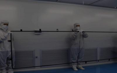
The International Consumer Electronics Show (CES) will be held online due to the corona crisis and will run January 11-14 this year. For the first time, CES will take place online this year. It has always been the leading trade fair for global consumer electronics, with exhibits ranging from small chips to large airplanes and yachts. The fair covers almost all consumer electronics products and the world’s largest companies typically present their latest products and show their latest technologies here.
Covalent Metrology Announces New FIB-SEM Services with Significant Advances in Imaging Resolution
The introduction of two cutting-edge dual-beam focused ion beam scanning electron (FIB-SEM) microscopes at Covalent’s Sunnyvale, CA headquarters will provide clients faster, deeper, and more advanced analytical capabilities.
Integrity Cleanroom has launched operations in the US and is now incorporated in Texas
Integrity Cleanroom is pleased to announce that it has begun commercial transactions with a brand new ecommerce platform and a dedicated team of professionals based in Texas.
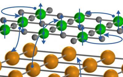
First detailed electronic study of new nickelate superconductor
The answers could help advance the synthesis of new unconventional superconductors and their use for power transmission, transportation and other applications, and also shed light on how the cuprates operate – which is still a mystery after more than 30 years of research.
PCB Piezotronics Completes $1M Cleanroom
PCB Piezotronics, Inc., a wholly owned subsidiary of MTS Systems Corporation (NASDAQ: MTSC), announced the completion of new environmentally controlled clean rooms totaling 4,300 sq. ft. at their Walden Avenue headquarters. Earlier this year, the sensor manufacturer began assembly of all pressure and force products in this new state-of-the-art facility.
Lockheed Martin’s Meridian, MS Facility Celebrates 50th Anniversary
Lockheed Martin’s Meridian facility began production operations in August 1969, initially producing the L-1011 jet airliner’s empennage. Since then, the Meridian facility has been involved in the production of aircraft components for the JetStar, the C-5 Galaxy and C-141 Starlifter strategic airlifters, the P-3 Orion submarine hunter, the F-22 Raptor fighter jet, and the C-130J Super Hercules tactical airlifter.
Hubbell Lighting Introduces SpectraClean™
Hubbell Lighting is elevating the lighting experience. Empowered by lighting solutions that integrate seamlessly into their environment, save energy, provide improved quality of light, deliver return on investment and armed with Hubbell’s unflinching support, its customers are able to think differently about how, where, and when they can use light.
Picosun Launches a new ALD Product Platform for up to 200 mm Wafer Markets
Picosun Group, the leading provider of AGILE ALD™ (Atomic Layer Deposition) thin film coating solutions, has launched PICOSUN™ Morpher, a new ALD product platform designed to disrupt the up to 200 mm wafer markets in Beyond and More than Moore domains.
Portable cleanroom system for contamination-free manufacturing
CAPE® is a transportable, tent-like cleanroom facility developed by researchers at the Fraunhofer Institute for Manufacturing Engineering and Automation IPA. It can be installed both indoors and in unexposed outdoor locations, and takes less than an hour to set up.
Clean Energy Grid to Benefit Communities
The PSC filing, including a five-year capital investment overview and detailed one-year plan for 2019, sets forth the projects Ameren Missouri plans to implement to modernize energy grid infrastructure in Missouri to benefit its customers and offer them more tools to manage their energy usage.
Lasers on Silicon Offer a Glimpse into the Future
Ten years into the future — that’s about how far UC Santa Barbara electrical and computer engineering professor John Bowers and his research team are reaching with the recent development of their mode-locked quantum dot lasers on silicon. It’s technology that not only can massively increase the data transmission capacity of data centers, telecommunications companies and network hardware products to come, but do so with high stability, low noise and the energy efficiency of silicon photonics.
QuantumClean® & ChemTrace® Show How to Reduce Wafer Fab CoO at SEMICON Europa 2018
QuantumClean & ChemTrace will demonstrate how its ultra-high purity chamber tool part cleaning, proprietary coatings and microcontamination analytical testing can help reduce wafer fabrication Cost-of-Ownership (CoO). Solutions’ information is available during show hours at SEMICON Europa at the Messe München Exhibition Center in Munich, Germany from November 13 — 16, 2018 (booth A4510).
Aerospace News
Optics Industry News and Advancements
The Optics Cleanroom Industry supports the environmental cleanroom and controlled environmental systems for the optics industry. The Optics Industry is the branch of physics that includes the behavior of light and the properties of light. This includes the way that light interacts with matter and the construction of optics instruments, optics products and optics technology that use light or detect light. Light is an electromagnetic wave which is very similar to other forms of electromagnetic radiation, like: x-rays, microwaves and radio waves.
Cleanroom Connect provides the latest Optics Industry News from various Optics Organizations, Optics Industries, and Optics Product Manufacturers. Subscribe today to receive optics news and updates directly to your mailbox.
Modern manufacturing is being revolutionized by the use of optics, which can both improve current manufacturing capabilities and enable new ones. Below are some of the uses of Optics in the industrial and product manufacturing landscapes:
- Light is often used to process or probe materials remotely, sometimes through windows isolating harsh or vacuum environments.
- Light can be used to induce photochemistry, for example, in photolithography to produce submicron features in thin films of photoresist or in rapid prototyping where liquid polymers are solidified by lasers to form a three-dimensional piece from a computer-aided design database.
- Light can cast images, making it possible to inspect a part or use the image to guide the working tool to the correct area of a production piece.
Optics has reached into every aspect of manufacturing and promises to increase in use with improvements in speed, control, precision, and accuracy. Numerous optical techniques are used throughout industry and are critical to the manufacture of such diverse and basic products as semiconductor chips, roads and tunnels, and chemicals. Optical techniques, grouped by function, fall into two broad classes:
-
Performing manufacturing: Light interacts directly with the finished or intermediate product to change its physical properties, as in the case of photolithography or materials processing.
-
Controlling manufacturing: Optics is used to provide information about a manufacturing process, as in the chemical industry’s use of optical sensors for in-line process control, or to inspect a manufactured
Keywords: Optics Industry, Optics News, Optics Industry News, Optics Organizations, Optics Industries, and Optics Product Manufacturers, Optics Research, Optics R&D, Optics Laboratory, Optics Cleanroom, x-rays, microwaves, radio waves
