Semiconductor Clean Room Industry Articles

GLOBALFOUNDRIES Breaks Ground On New Fab In Singapore

GLOBALFOUNDRIES® (GF®), the global leader in feature-rich semiconductor manufacturing, today announced it is expanding its global manufacturing footprint with the construction of a new fab on its Singapore campus. In partnership with the Singapore Economic Development Board and with co-investments from committed customers, GF’s more than US $4B (S$5B) investment will play an integral role in meeting the growing demand for the company’s industry-leading manufacturing technologies and services to enable companies worldwide to develop and scale their business.

Intel to Invest $3.5 Billion to Expand New Mexico Manufacturing Operations

Intel Corporation will invest $3.5 billion to equip its New Mexico operations for the manufacturing of advanced semiconductor packaging technologies, including Foveros, Intel’s breakthrough 3D packaging technology. The multiyear investment is expected to create at least 700 high-tech jobs and 1,000 construction jobs and support an additional 3,500 jobs in the state. Planning activities begin immediately, with construction expected to start in late 2021.

Bosch reaches milestone on the way to opening new wafer fab in Dresden

It is a milestone on the path to the chip factory of the future: at the new Bosch semiconductor fab in Dresden, silicon wafers are passing through the fully automated fabrication process for the first time. This is a key step toward the start of production operations, which is scheduled for late 2021. Manufacturing of automotive microchips will be a primary focus when the fully digital and highly connected semiconductor plant is up and running. “Chips for tomorrow’s mobility solutions and greater safety on our roads will soon be produced in Dresden. We plan to open our chip factory of the future before the year is out,” says Harald Kroeger, member of the board of management of Robert Bosch GmbH. The company already operates a semiconductor fab in Reutlingen near Stuttgart. The new wafer fab in Dresden is Bosch’s response to the surging number of areas of application for semiconductors, as well as a renewed demonstration of its commitment to Germany as a high-tech location. Bosch is investing around one billion euros in the high-tech manufacturing facility, which will be one of the most advanced wafer fabs in the world. Funding for the new building is being provided by the federal German government, and more specifically the Federal Ministry for Economic Affairs and Energy. Bosch plans to officially open its wafer fab in June 2021.

Cinotop & Micron presents “Touch Everywhere” at The International Consumer Electronics Show

The International Consumer Electronics Show (CES) will be held online due to the corona crisis and will run January 11-14 this year. For the first time, CES will take place online this year. It has always been the leading trade fair for global consumer electronics, with exhibits ranging from small chips to large airplanes and yachts. The fair covers almost all consumer electronics products and the world’s largest companies typically present their latest products and show their latest technologies here.

Global Semiconductor Sales Increase 29.2% Year-to-Year

Global Semiconductor Sales Increase 29.2% Year-to-Year

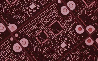
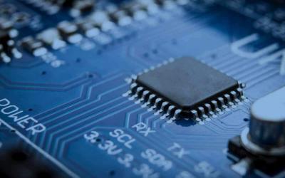
The Semiconductor Industry Association (SIA) today announced worldwide sales of semiconductors were $44.5 billion in June 2021, an increase of 29.2% from the June 2020 total of $34.5 billion. Sales in June were 2.1% more than the May 2021 total of $43.6 billion. Sales during the second quarter of 2021 were $133.6 billion, an increase of 29.2% over the second quarter of 2020 and 8.3% more than the first quarter of 2021. Monthly sales are compiled by the World Semiconductor Trade Statistics (WSTS) organization and represent a three-month moving average. SIA represents 98% of the U.S. semiconductor industry by revenue and nearly two-thirds of non-U.S. chip firms.

read more
Micron Launches World’s First 176-Layer NAND in Mobile Solutions to Power Lightning-Fast 5G Experiences

Micron Launches World’s First 176-Layer NAND in Mobile Solutions to Power Lightning-Fast 5G Experiences

Micron Technology, Inc., announced today it has begun volume shipments of the world’s first 176-layer NAND Universal Flash Storage (UFS) 3.1 mobile solution. Engineered for high-end and flagship phones, Micron’s discrete UFS 3.1 mobile NAND unlocks 5G’s potential with up to 75% faster sequential write and random read performance than prior generations,1 enabling downloads of two-hour 4K movies2 in as little as 9.6 seconds.

read more
Nanomaterial Superconductivity Lost? Physicists Uncover Why

Nanomaterial Superconductivity Lost? Physicists Uncover Why

Scientists discovered the phenomenon 30 years ago, but the mechanism for superconductivity remains an enigma because the majority of materials are too complex to understand QPT physics in details. A good strategy would be first to look at less complicated model systems.

read more
Quantum Transistor for Semiconductor Applications Enables Photon Computing

Quantum Transistor for Semiconductor Applications Enables Photon Computing

Quantum computers will need analogous hardware to manipulate quantum information. But the design constraints for this new technology are stringent, and today’s most advanced processors can’t be repurposed as quantum devices. That’s because quantum information carriers, dubbed qubits, have to follow different rules laid out by quantum physics.

read more
Indium Oxide Nanocrystals Comprise New UV Narrow-Band Photodetector

Indium Oxide Nanocrystals Comprise New UV Narrow-Band Photodetector

Semiconductor quantum dots (nanocrystals just a few nanometers in size) have attracted researchers’ attention due to the size dependent effects that determine their novel electrical and optical properties. By changing the size of such objects, it is possible to adjust the wavelength of the emission they absorb, thus implementing selective photodetectors, including those for UV radiation.

read more
Biosensor Chips based on Copper and Graphene Oxide

Biosensor Chips based on Copper and Graphene Oxide

Russian researchers from the Moscow Institute of Physics and Technology have developed biosensor chips of unprecedented sensitivity, which are based on copper instead of the conventionally used gold. Besides making the device somewhat cheaper, this innovation will facilitate the manufacturing process.

read more