by MITRE Engenuity
The Semiconductor Alliance have joined together to create a vision and path for a more resilient and innovation-focused semiconductor supply chain, one that ensures American innovation truly leads to American growth.

by ATREG Inc.
ATREG, Inc. has successfully advised Texas Instruments (TI) on the acquisition of Micron’s operational 300mm fab located in Lehi, UT. The transaction previously announced in June 2021 for $900 million has closed.

by Siltronic
Siltronic, one of the technology leaders in silicon wafer manufacturing, broke ground for its new manufacturing facility at JTC’s Tampines Wafer Fab Park in Singapore.

by JinkoSolar Holding Co., Ltd.
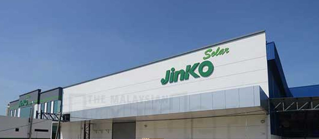
JinkoSolar Holding Co., Ltd. (“JinkoSolar” or the “Company”) (NYSE: JKS), one of the largest and most innovative solar module manufacturers in the world, today announced that the Company is investing $500 million to build a monocrystalline ingot and wafer manufacturing facility in Quảng Ninh Province, Vietnam.

by Semiconductors Industry Association
The Semiconductor Industry Association (SIA) today announced worldwide sales of semiconductors were $44.5 billion in June 2021, an increase of 29.2% from the June 2020 total of $34.5 billion. Sales in June were 2.1% more than the May 2021 total of $43.6 billion. Sales during the second quarter of 2021 were $133.6 billion, an increase of 29.2% over the second quarter of 2020 and 8.3% more than the first quarter of 2021. Monthly sales are compiled by the World Semiconductor Trade Statistics (WSTS) organization and represent a three-month moving average. SIA represents 98% of the U.S. semiconductor industry by revenue and nearly two-thirds of non-U.S. chip firms.

by Micron Technology, Inc.
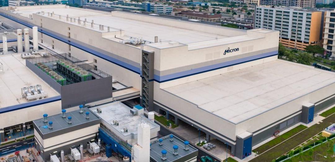
Micron Technology, Inc., announced today it has begun volume shipments of the world’s first 176-layer NAND Universal Flash Storage (UFS) 3.1 mobile solution. Engineered for high-end and flagship phones, Micron’s discrete UFS 3.1 mobile NAND unlocks 5G’s potential with up to 75% faster sequential write and random read performance than prior generations,1 enabling downloads of two-hour 4K movies2 in as little as 9.6 seconds.

by Picosun Oy
Picosun Group delivers cutting-edge Atomic Layer Deposition (ALD) technology to ams OSRAM for volume manufacturing of optical semiconductor devices…

by ClassOne Technology
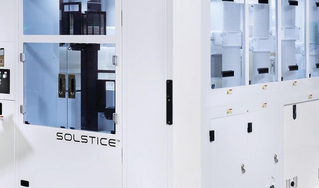
ClassOne Technology, global provider of advanced semiconductor electroplating and surface preparation systems, announced that it has received multiple tool orders from one of the world’s largest RF device manufacturers…

by GlobalFoundries
GlobalFoundries (GF), the global leader in feature-rich semiconductor manufacturing, today announced its expansion plans for its most advanced manufacturing facility in upstate New York over the coming years. These plans include immediate investments to address the global chip shortage at its existing Fab 8 facility as well as construction of a new fab on the same campus that will double the site’s capacity.

by GLOBALFOUNDRIES
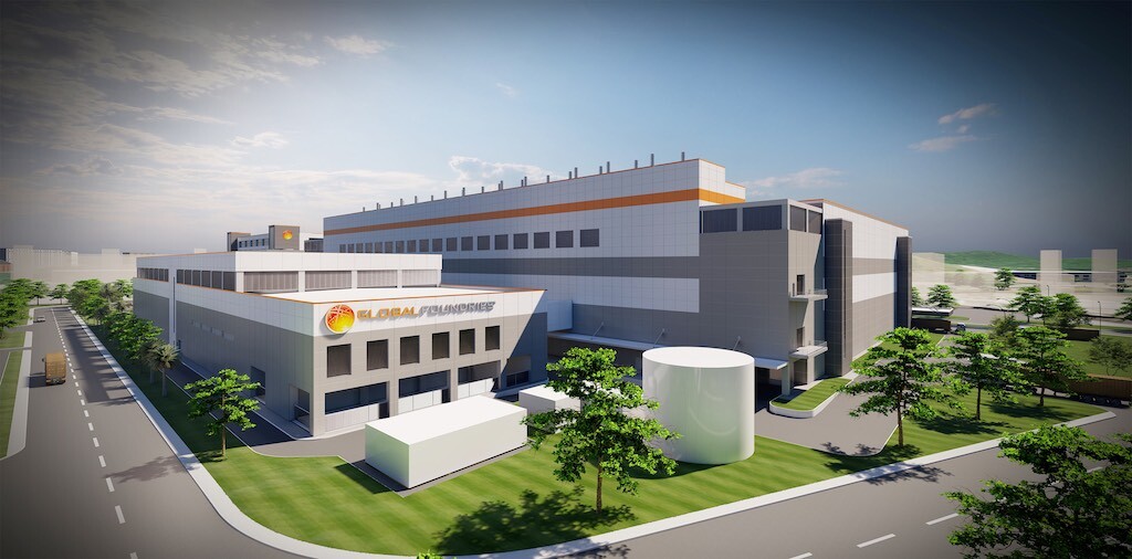
GLOBALFOUNDRIES® (GF®), the global leader in feature-rich semiconductor manufacturing, today announced it is expanding its global manufacturing footprint with the construction of a new fab on its Singapore campus. In partnership with the Singapore Economic Development Board and with co-investments from committed customers, GF’s more than US $4B (S$5B) investment will play an integral role in meeting the growing demand for the company’s industry-leading manufacturing technologies and services to enable companies worldwide to develop and scale their business.

by SkyWater Technology
SkyWater Technology, the trusted technology realization partner, today announced it has entered into an exclusive, non-binding Memorandum of Understanding (MOU) with Osceola County, Florida to explore taking over the lease of the Center for Neovation, a state-of-the-art 200 mm semiconductor manufacturing facility, by forming a new public-private partnership for microelectronics manufacturing and advanced packaging capabilities. Following the MOU, SkyWater, the only U.S

by Cardiff University - Institute for Compound Semiconductors
Local business leaders across South Wales attended the launch of the new facility, which offers a range of solutions for companies working to develop 21st century technologies. Guests were able to learn more about the refurbished 225 square metre Clean Room facility and the role it plays in assisting businesses across South Wales as part of CS Connected – the world’s first Compound Semiconductor cluster.

