by GlobalFoundries
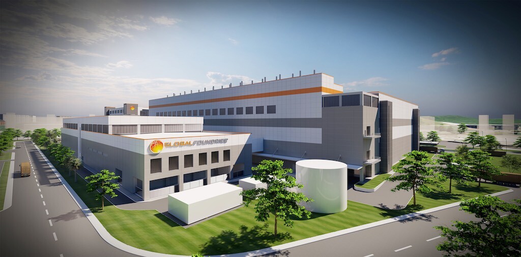
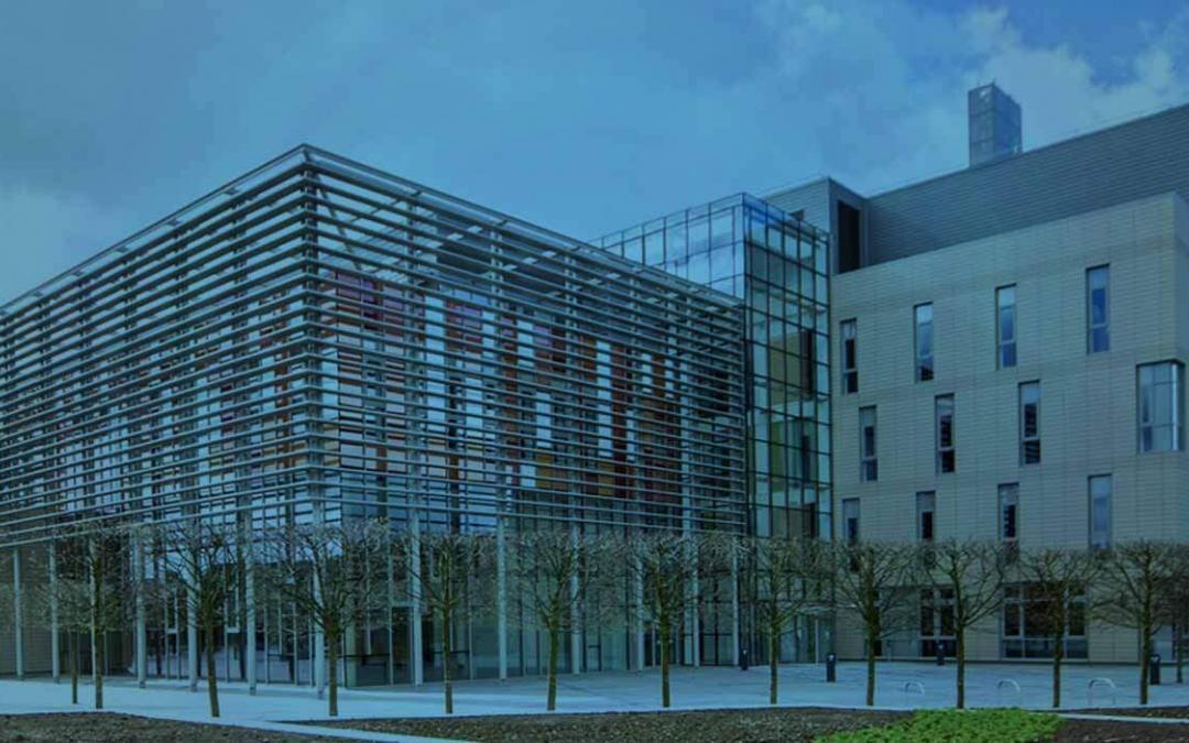
GlobalFoundries (GF), the global leader in feature-rich semiconductor manufacturing, today announced its expansion plans for its most advanced manufacturing facility in upstate New York over the coming years. These plans include immediate investments to address the global chip shortage at its existing Fab 8 facility as well as construction of a new fab on the same campus that will double the site’s capacity.
by GLOBALFOUNDRIES
GLOBALFOUNDRIES® (GF®), the global leader in feature-rich semiconductor manufacturing, today announced it is expanding its global manufacturing footprint with the construction of a new fab on its Singapore campus. In partnership with the Singapore Economic Development Board and with co-investments from committed customers, GF’s more than US $4B (S$5B) investment will play an integral role in meeting the growing demand for the company’s industry-leading manufacturing technologies and services to enable companies worldwide to develop and scale their business.

by SkyWater Technology
SkyWater Technology, the trusted technology realization partner, today announced it has entered into an exclusive, non-binding Memorandum of Understanding (MOU) with Osceola County, Florida to explore taking over the lease of the Center for Neovation, a state-of-the-art 200 mm semiconductor manufacturing facility, by forming a new public-private partnership for microelectronics manufacturing and advanced packaging capabilities. Following the MOU, SkyWater, the only U.S
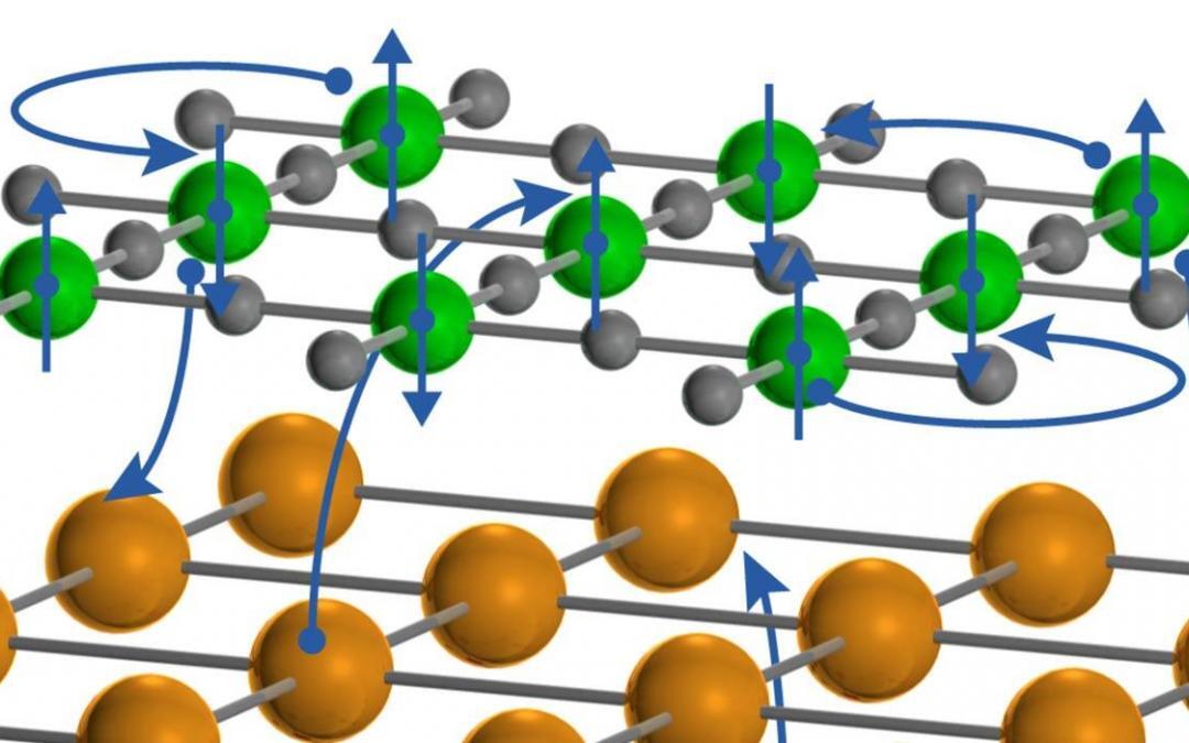
by GLENNDA CHUI - SLAC NATIONAL ACCELERATOR LABORATORY
The answers could help advance the synthesis of new unconventional superconductors and their use for power transmission, transportation and other applications, and also shed light on how the cuprates operate – which is still a mystery after more than 30 years of research.
by SK Hynix
SK hynix has grown into one of the leading chipmakers in the world through continuous effort to secure a fundamental competitive edge in the fierce semiconductor industry. With the emergence of new entrants and the consolidation of incumbent players, the competition and technological barriers are continuously heightening in the market.
by Cardiff University - Institute for Compound Semiconductors
Local business leaders across South Wales attended the launch of the new facility, which offers a range of solutions for companies working to develop 21st century technologies. Guests were able to learn more about the refurbished 225 square metre Clean Room facility and the role it plays in assisting businesses across South Wales as part of CS Connected – the world’s first Compound Semiconductor cluster.
by Infineon
Infineon Technologies AG is to build a new factory for power semiconductors. The market and technology leader in this segment will thereby create the foundation for long-term, profitable growth. A fully automated chip factory for manufacturing 300-millimeter thin wafers will be constructed at the Villach location in Austria alongside the existing production facility. Austria’s Chancellor Sebastian Kurz, Dr. Reinhard Ploss, Chief Executive Officer of Infineon, and Dr. Sabine Herlitschka, Chief Executive Officer of Infineon Austria, presented the project in Vienna.

by Area Development News Desk
II-VI EpiWorks opened an expansion of its center of manufacturing excellence in Champaign, Illinois. The company’s state-of-the-art facility is a manufacturing center for compound semiconductors that makes epitaxial wafer products. The expansion will quadruple production of products that enable some of the most exciting new consumer electronics in the world.
by Cleanroom Connect Editor
GlobalFoundries Fab plans for the upcoming year display the company’s urge to be a leader in the semiconductor market and to provide a strong position in the Chinese and global economies. Tom Caulfield, the new CEO of GlobalFoundries has a plan to improve financial performance of the privately held chipmaker. Therefore, GlobalFoundries is seeking partners to help Global Foundries be a strong competitor in the hot chip market.

by Micron Technology, Inc.
Semiconductor giant Micron Technology broke ground in North Coast yesterday to add new cleanroom space for production of its 3D NAND flash memory products. Micron did not disclose the cost, except to say that the new facility will be a “multi-billion- dollar investment”. It will be equipped over the next five years or more and add 1,000 new jobs in Singapore. As part of its agreement with the Economic Development Board, Micron will also broaden its research and development (R&D) capabilities here. The 1,000 new roles it is adding will comprise mainly engineers and technicians related to R&D and manufacturing.

by Cleanroom Connect Editor
Radar and 5G Applications by GlobalFoundries. The RFwave Partner Program builds upon GF’s 5G vision and roadmap, with a focus on the company’s industry-leading radio frequency (RF) solutions, such as FD-SOI, RF CMOS (bulk and advanced CMOS nodes), RF SOI and silicon germanium (SiGe) technologies.
by Cleanroom Connect Editor
The new mobile 3D NAND flash products pack more storage cells into a smaller die area, and by utilizing Micron’s CMOS under Array (CuA), they deliver a best-in-class die size. Micron’s unique approach places all the flash memory layers on top of the logic array, maximizing the use of space in the smartphone design.