by Advanced Science News
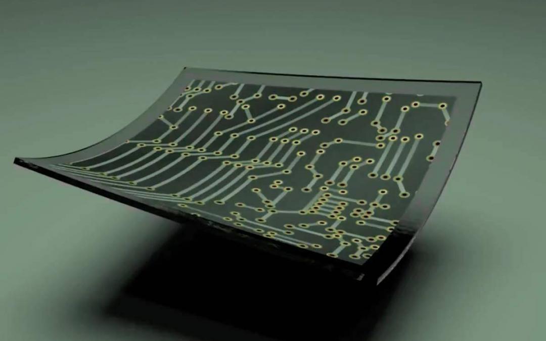
A flexible, durable and solvent-resistance inorganic polymer. (Allylhybridpolycarbosilane or AHPCS) was used to fabricate the microstructured AHPCS shearing blade. The wet-ability of the AHPCS micropillar surface is tunable. By controlling the shearing rate and the substrate temperature, crystal growth can occur along the moving blade.

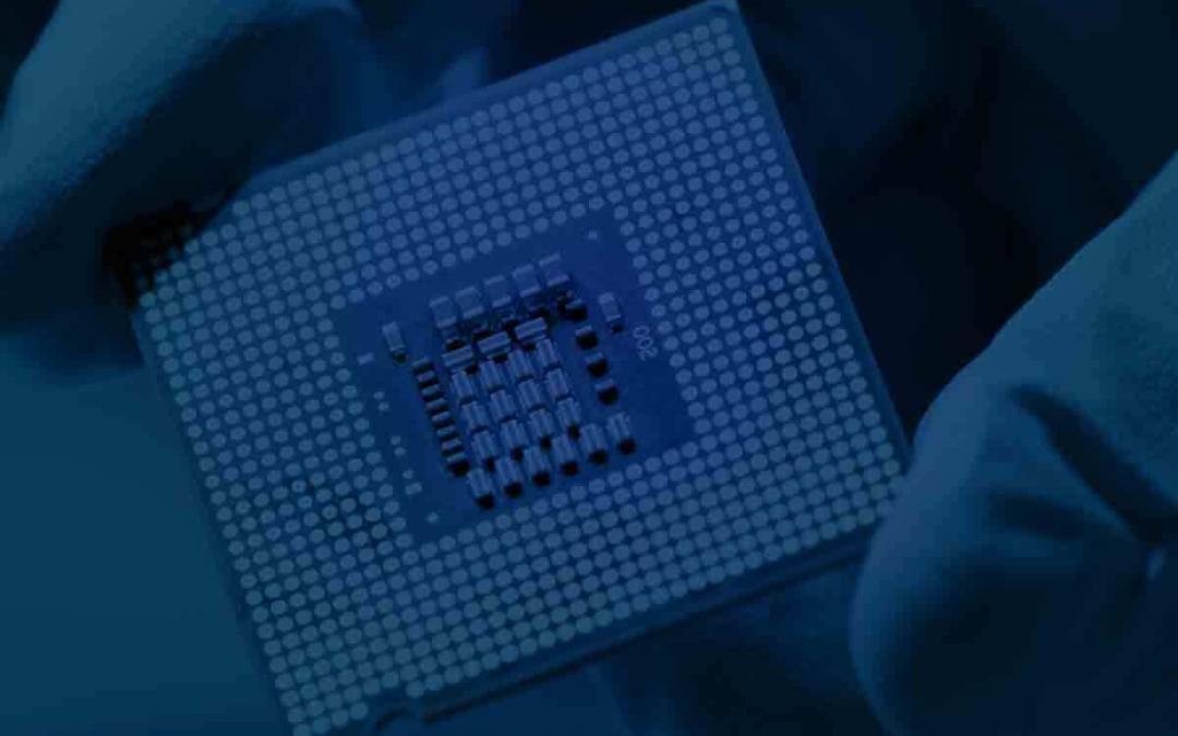
by ON Semiconductor
ON Semiconductor Corporation (Nasdaq: ON), driving energy efficient innovations, is excited to announce the expansion of their manufacturing facility in Rochester, New York. The site develops and manufactures image sensor devices for commercial, industrial and professional imaging applications, including machine vision, surveillance, traffic monitoring, medical and scientific imaging and photography.
by Gene Stowe | University of Notre Dame
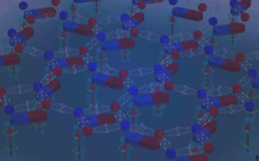
New Superconductor Design presents a better superconductor with geometric frustration. Superconductors contain tiny tornadoes of supercurrent, called vortex filaments, that create resistance when they move. This affects the way superconductors carry a current. A new superconductor design creates potential making them better for applications.

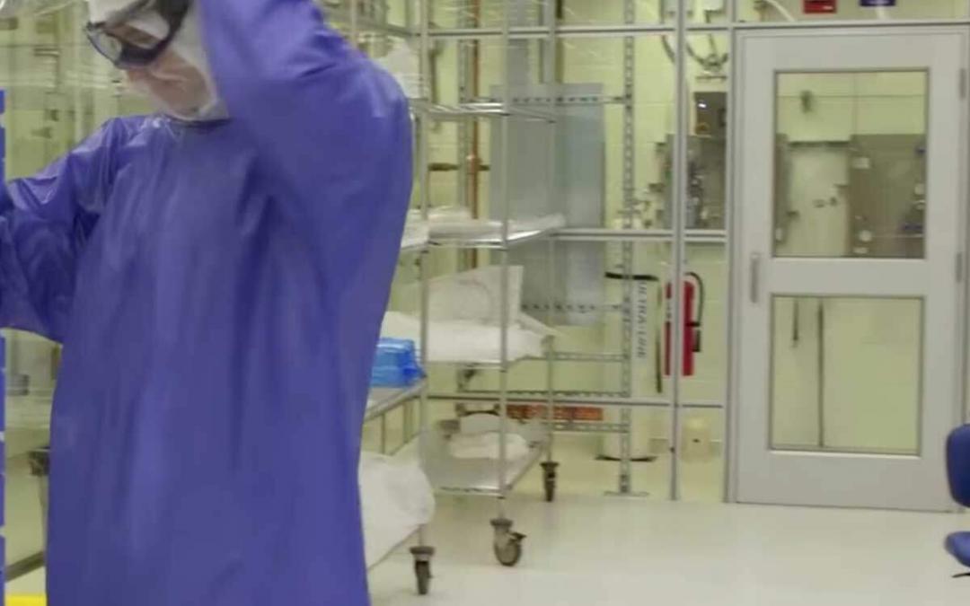
by Micron Technology, Inc.
Micron shares their process for memory chip fabrication in their state-of-the-art nanofab cleanrooms
From laptops to mobile phones to connected cars and homes, memory and storage are helping change how the world works, plays, communicates and connects. Check out this behind the scenes look at Micron’s state of the art fabrication process for how memory chips are made – from initial design all the way through testing and packaging.
by Cleanroom Connect Editor
GlobalFoundries Fab plans for the upcoming year display the company’s urge to be a leader in the semiconductor market and to provide a strong position in the Chinese and global economies. Tom Caulfield, the new CEO of GlobalFoundries has a plan to improve financial performance of the privately held chipmaker. Therefore, GlobalFoundries is seeking partners to help Global Foundries be a strong competitor in the hot chip market.

by Cleanroom Connect Editor
ON Semiconductor Corporation, driving energy efficient innovations, is excited to announce the expansion of their manufacturing facility in Rochester, New York. The site develops and manufactures image sensor devices for commercial, industrial and professional imaging applications, including machine vision, surveillance, traffic monitoring, medical and scientific imaging and photography.
by Cleanroom Connect Editor
NYU Tandon Cleanroom for Advancing Technology – The NYU Tandon School of Engineering today will preview Brooklyn’s first NYU Tandon Cleanroom for Advancing Technology, where scientists and engineers from across greater New York will fabricate advanced materials and devices on the micro- and nano-scale in order to push the boundaries of established scientific principles and future technology. Such fabrication facilities are essential to experiments in nanotechnology, quantum computing, minute biosensors that could revolutionize medicine, ultra-fast electronics, hardware that is secure from hackers, and much more.

by Micron Technology, Inc.
Semiconductor giant Micron Technology broke ground in North Coast yesterday to add new cleanroom space for production of its 3D NAND flash memory products. Micron did not disclose the cost, except to say that the new facility will be a “multi-billion- dollar investment”. It will be equipped over the next five years or more and add 1,000 new jobs in Singapore. As part of its agreement with the Economic Development Board, Micron will also broaden its research and development (R&D) capabilities here. The 1,000 new roles it is adding will comprise mainly engineers and technicians related to R&D and manufacturing.
by ASU
The new ASU Nanotechnology Facility is open to students, faculty and staff researchers, as well as government, and industrial partners, the ASU Nanotechnology Facility offers a comprehensive set of tools to develop new micro and nanoscale devices, such as integrated circuits, nanophotonic and solid state devices, micro-electromechanical systems, and microfluidic systems, among others. The NanoFabrication Facility also offers students and researchers some of the most advanced instruments for fabrication and characterization of materials at the micro and nanoscales.

by Cleanroom Connect Editor
Radar and 5G Applications by GlobalFoundries. The RFwave Partner Program builds upon GF’s 5G vision and roadmap, with a focus on the company’s industry-leading radio frequency (RF) solutions, such as FD-SOI, RF CMOS (bulk and advanced CMOS nodes), RF SOI and silicon germanium (SiGe) technologies.

by Cleanroom Connect Editor
Oxide electronics materials boast a wide array of behaviors, including electronic, magnetic and superconducting, oxide electronics materials are poised to expand the way we think about the functions of traditional silicon-based electronic devices such as cell phones or computers.
by University of Chicago
The Pritzker Foundation provided a generous a $15 million gift to develop the 10,000 square foot large nanofacility for the University of Chicago. The National Science Foundation provided an additional $5 million to establish the Soft and Hybrid Nanotechnology Experimental Resource, a partnership between UChicago and Northwestern University.