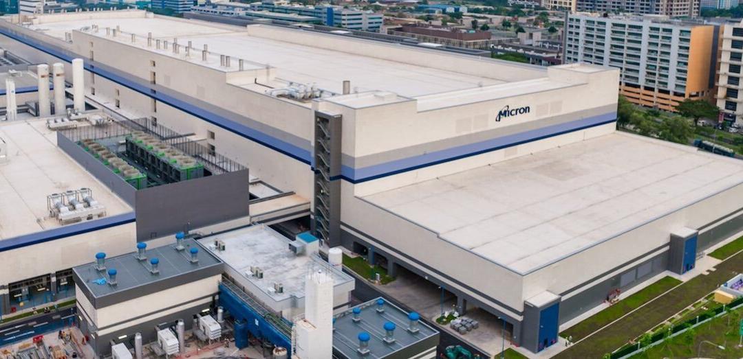
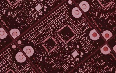
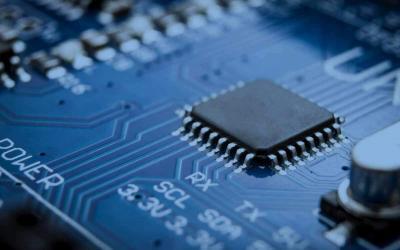
Picosun Group delivers cutting-edge Atomic Layer Deposition (ALD) technology to ams OSRAM for volume manufacturing of optical semiconductor devices…

Picosun Group delivers cutting-edge Atomic Layer Deposition (ALD) technology to ams OSRAM for volume manufacturing of optical semiconductor devices…
ClassOne Technology, global provider of advanced semiconductor electroplating and surface preparation systems, announced that it has received multiple tool orders from one of the world’s largest RF device manufacturers…
GlobalFoundries (GF), the global leader in feature-rich semiconductor manufacturing, today announced its expansion plans for its most advanced manufacturing facility in upstate New York over the coming years. These plans include immediate investments to address the global chip shortage at its existing Fab 8 facility as well as construction of a new fab on the same campus that will double the site’s capacity.
Smart bandages designed to monitor and tailor treatment for chronic wounds Smart Bandages with integrated pH and...
UT Dallas physics researchers recently published a study in the journal Science that describes the high thermal conductivity of boron arsenide crystals they grew in the lab. From left: study authors Xiaoyuan Liu, Dr. Bing Lv and Dr. Sheng Li.
Quantum computers will need analogous hardware to manipulate quantum information. But the design constraints for this new technology are stringent, and today’s most advanced processors can’t be repurposed as quantum devices. That’s because quantum information carriers, dubbed qubits, have to follow different rules laid out by quantum physics.
Nanoscale Kirigami has taken off as a field of research in the last few years; the approach is based on the ancient arts of origami (making 3-D shapes by folding paper) and kirigami (which allows cutting as well as folding) but applied to flat materials at the nanoscale, measured in billionths of a meter.
NexLogic Technologies, Inc. has announced the completion of its International Standards Organization (ISO) 14644-1 Class 4/10,000 and the equivalent Federal Standard 209E (FS209E) Class 10 clean room as an integral part of its new microelectronics services and manufacturing capability.
Semiconductor quantum dots (nanocrystals just a few nanometers in size) have attracted researchers’ attention due to the size dependent effects that determine their novel electrical and optical properties. By changing the size of such objects, it is possible to adjust the wavelength of the emission they absorb, thus implementing selective photodetectors, including those for UV radiation.
Russian researchers from the Moscow Institute of Physics and Technology have developed biosensor chips of unprecedented sensitivity, which are based on copper instead of the conventionally used gold. Besides making the device somewhat cheaper, this innovation will facilitate the manufacturing process.
Invigorating the idea of computers based on fluids instead of silicon, researchers at the National Institute of Standards and Technology (NIST) have shown how computational logic operations could be performed in a liquid medium by simulating the trapping of ions (charged atoms) in graphene (a sheet of carbon atoms) floating in saline solution. The scheme might also be used in applications such as water filtration, energy storage or sensor technology.
A team of researchers from the Department of Energy’s Lawrence Berkeley National Laboratory (Berkeley Lab) and UC Berkeley are developing innovative machine learning tools to pull contextual information from scientific datasets and automatically generate metadata tags for each file. Scientists can then search these files via a web-based search engine for scientific data, called Science Search, that the Berkeley team is building.