Stellantis N.V. and Samsung SDI announced that they have executed binding, definitive agreements to establish an electric-vehicle battery manufacturing facility in Kokomo, Indiana.
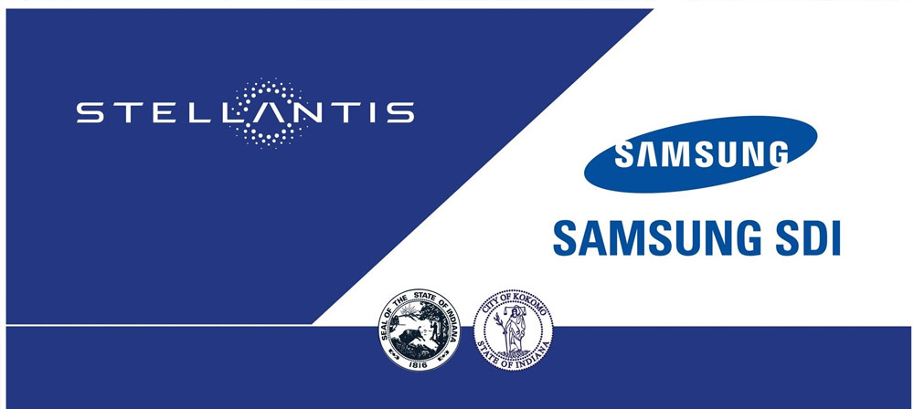
Stellantis and Samsung SDI to Invest Over $2.5 Billion in Joint Venture for Lithium-ion Battery Production Plant in United States
read more