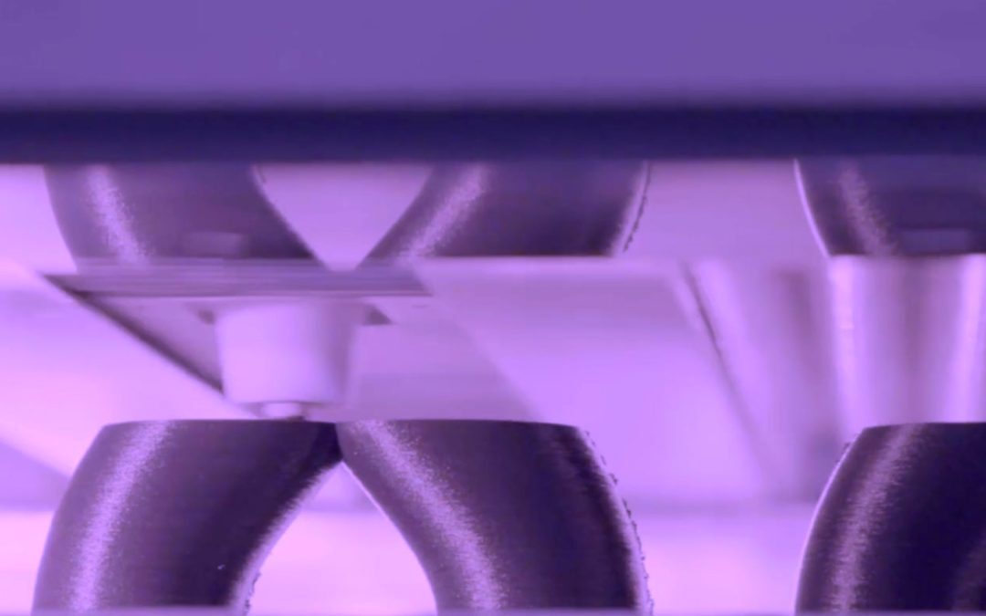
Essentium Introduces Industry-First Anti-Static Material To Advance Additive Manufacturing Applications In The Aerospace And Defense Industries


Essentium Introduces Industry-First Anti-Static Material To Advance Additive Manufacturing Applications In The Aerospace And Defense Industries

Purolite Corporation is expanding its manufacturing capabilities to address and fulfill the increasing global demand for its pharmaceutical and life science products. The new facility will include two new cleanrooms to manufacture active pharmaceutical ingredients (APIs) and excipients and an agarose manufacturing facility equipped with proprietary jetting technology for the capture and purification of (mAbs) monoclonal antibodies sold under the Praesto® brand.

SkyWater Technology, the trusted technology realization partner, today announced it has entered into an exclusive, non-binding Memorandum of Understanding (MOU) with Osceola County, Florida to explore taking over the lease of the Center for Neovation, a state-of-the-art 200 mm semiconductor manufacturing facility, by forming a new public-private partnership for microelectronics manufacturing and advanced packaging capabilities. Following the MOU, SkyWater, the only U.S
UCLA scientists and engineers have developed a new semiconductor assembly process. The advance could lead to much more energy-efficient transistors for electronics and computer chips, diodes for solar cells and light-emitting diodes, and other semiconductor-based devices.
Researchers have demonstrated large-scale fabrication of a new type of transparent conductive electrode film based on nanopatterned silver. Smartphone touch screens and flat panel televisions use transparent electrodes to detect touch and to quickly switch the color of each pixel.
Micron shares their process for memory chip fabrication in their state-of-the-art nanofab cleanrooms
From laptops to mobile phones to connected cars and homes, memory and storage are helping change how the world works, plays, communicates and connects. Check out this behind the scenes look at Micron’s state of the art fabrication process for how memory chips are made – from initial design all the way through testing and packaging.
Led by Drs Andrij Vasylenko, Samuel Marks, Jeremy Sloan and David Quigley from Warwick’s Department of Physics, in collaboration with the Universities of Cambridge and Birmingham, the researchers have found that the most effective thermoelectric materials can be realised by shaping them into the thinnest possible nanowires.
Infineon Technologies AG is to build a new factory for power semiconductors. The market and technology leader in this segment will thereby create the foundation for long-term, profitable growth. A fully automated chip factory for manufacturing 300-millimeter thin wafers will be constructed at the Villach location in Austria alongside the existing production facility. Austria’s Chancellor Sebastian Kurz, Dr. Reinhard Ploss, Chief Executive Officer of Infineon, and Dr. Sabine Herlitschka, Chief Executive Officer of Infineon Austria, presented the project in Vienna.
II-VI EpiWorks opened an expansion of its center of manufacturing excellence in Champaign, Illinois. The company’s state-of-the-art facility is a manufacturing center for compound semiconductors that makes epitaxial wafer products. The expansion will quadruple production of products that enable some of the most exciting new consumer electronics in the world.
Atomic-scale manufacturing revolutionizes the future of electronics production. The University of Alberta Scientists have innovated an atomic-scale manufacturing process, setting a standard for mass production of electronics that are faster, smaller and consume less energy than the electronics of today. The implications of this new atomic-scale manufacturing capability are enormous. In the future, we will see mobile phones that can go months without a charge and computers that are faster (100X) but use 1/1000th of the power currently used for device operation.
The IoT network of interconnected devices is Ubiquitous. IoT will reach far beyond the expected computers and mobile devices. Companies will be innovating and creating new technology, products, infrastructure solutions, and data storage solutions to stay at the forefront of this vast network. The 2018 Semiconductor Market is one that will see continued growth due to the increased need for data storage, memory and speed.
How will semiconductor companies follow such remarkable performance in 2018? Many of the leaders in the semiconductor industry foresee growth in revenue and product segmentation in the 2018 Semiconductor Market. Semiconductors are a $412 billion global industry and encompasses products such as sensors, microprocessors and memory devices. Since these are the building blocks of all modern technology, trends and innovation in semiconductors have a direct impact on all downstream technologies.