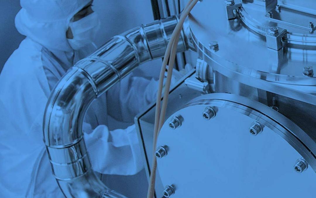
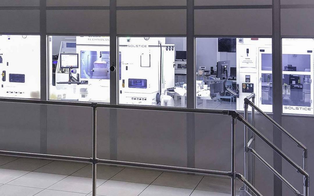
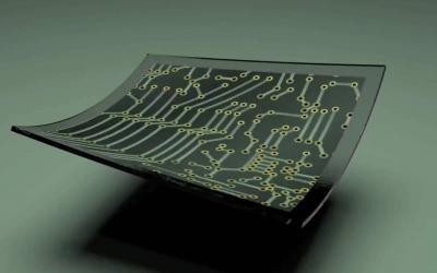
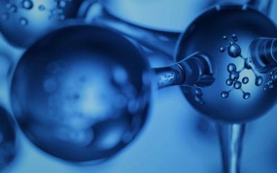
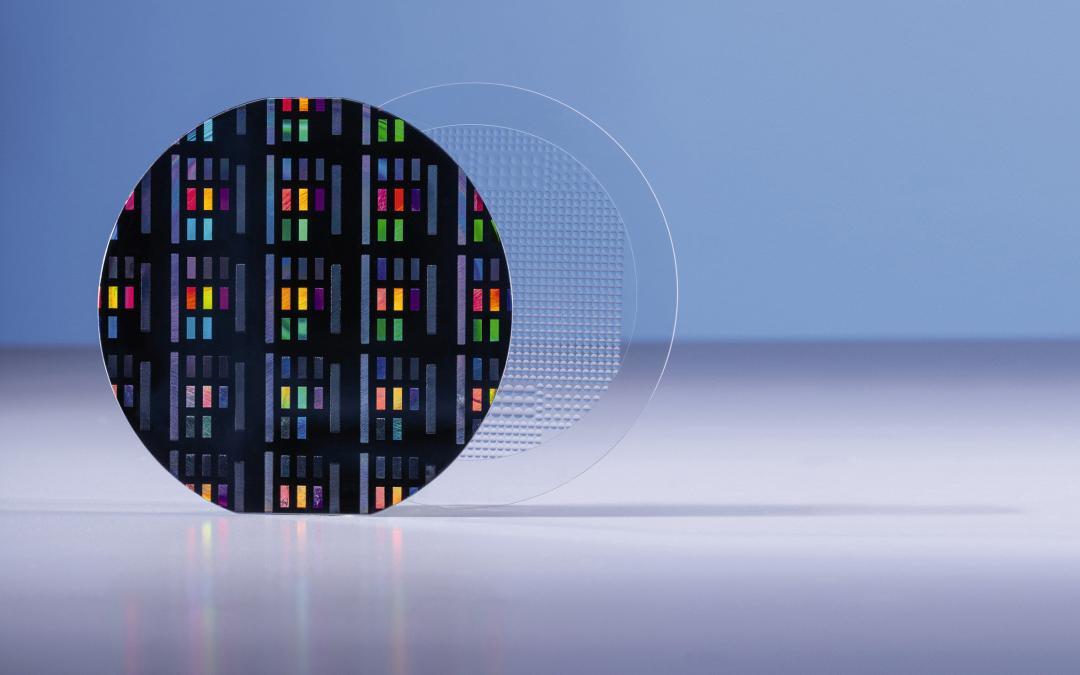
Nanotechnology Clean Room Industry Articles

Rebar Graphene Material Proves To Be Twice As Tough

In a new study in the American Chemical Society journal ACS Nano, Rice materials scientist Jun Lou, graduate student and lead author Emily Hacopian and collaborators, including Tour, stress-tested rebar graphene and found that nanotube rebar diverted and bridged cracks that would otherwise propagate in unreinforced graphene.

BiCS Flash fab Development kickoff by Toshiba

Demand for 3D flash memory is increasing significantly on fast growing demand for enterprise servers, datacenters and smartphones. Toshiba memory expects continued strong growth in the mid and long term. The new facility will make a major contribution to business competitiveness in corporation with Yokkaichi operations.

New Semiconductor Fab Prepares SK Hynix for Increasing Memory Demand

SK hynix has grown into one of the leading chipmakers in the world through continuous effort to secure a fundamental competitive edge in the fierce semiconductor industry. With the emergence of new entrants and the consolidation of incumbent players, the competition and technological barriers are continuously heightening in the market.

New Biosensors For Implantable Sensing

Biosensors are devices that can detect biological molecules in air, water, or blood. They are widely used in drug development, medical diagnostics, and biological research. The growing need for continuous, real-time monitoring of biomarkers in diseases like diabetes is currently driving efforts to develop efficient and portable biosensor devices.

Particle Robotic System

Particle Robotic System

Taking a cue from biological cells, researchers from MIT, Columbia University, and elsewhere have developed computationally simple robots that connect in large groups to move around, transport objects, and complete other tasks.

read more
Nano Decorations Remove Water Contaminants

Nano Decorations Remove Water Contaminants

A Recent Study Shows how Grains of Sediment and Nano Decorations Capture & Release Impurities in Water. When bacteria and viruses get into well water and make people sick, often the contamination comes after heavy rain or flooding. In 2000, more than 2,300 people in Walkerton, Ontario, got sick when, after unusually heavy rains. E. coli bacteria found their way to drinking water wells. Seven people died.

read more
Dialog Semiconductor Enters Growing Haptics Market

Dialog Semiconductor Enters Growing Haptics Market

Dialog Semiconductor, a provider of highly integrated power management, AC/DC power conversion, charging, and Bluetooth® low energy technology, today unveiled the DA7280, a new Haptic Driver Integrated Circuit (IC). The device is capable of driving both ERM (Eccentric Rotating Mass) and LRA (Linear Resonant Actuators) motors

read more
Center for Neovation in Neocity

Center for Neovation in Neocity

Intensely focused on the future, the Center for Neovation, formerly known as the Florida Advanced Manufacturing Research Center (FAMRC) was designed and constructed in 24 months.

read more
Semiconductor Manufacturing Facility Expansion

Semiconductor Manufacturing Facility Expansion

ON Semiconductor Corporation (Nasdaq: ON), driving energy efficient innovations, is excited to announce the expansion of their manufacturing facility in Rochester, New York. The site develops and manufactures image sensor devices for commercial, industrial and professional imaging applications, including machine vision, surveillance, traffic monitoring, medical and scientific imaging and photography.

read more
New Superconductor Design allows for better control at the nanoscale

New Superconductor Design allows for better control at the nanoscale

New Superconductor Design presents a better superconductor with geometric frustration. Superconductors contain tiny tornadoes of supercurrent, called vortex filaments, that create resistance when they move. This affects the way superconductors carry a current. A new superconductor design creates potential making them better for applications.

read more
New Semiconductor Assembly Process

New Semiconductor Assembly Process

UCLA scientists and engineers have developed a new semiconductor assembly process. The advance could lead to much more energy-efficient transistors for electronics and computer chips, diodes for solar cells and light-emitting diodes, and other semiconductor-based devices.

read more
Evolving Flexible Screen Technology

Evolving Flexible Screen Technology

Researchers have demonstrated large-scale fabrication of a new type of transparent conductive electrode film based on nanopatterned silver. Smartphone touch screens and flat panel televisions use transparent electrodes to detect touch and to quickly switch the color of each pixel.

read more
Memory Chip Fabrication Process

Memory Chip Fabrication Process

Micron shares their process for memory chip fabrication in their state-of-the-art nanofab cleanrooms
From laptops to mobile phones to connected cars and homes, memory and storage are helping change how the world works, plays, communicates and connects. Check out this behind the scenes look at Micron’s state of the art fabrication process for how memory chips are made – from initial design all the way through testing and packaging.

read more