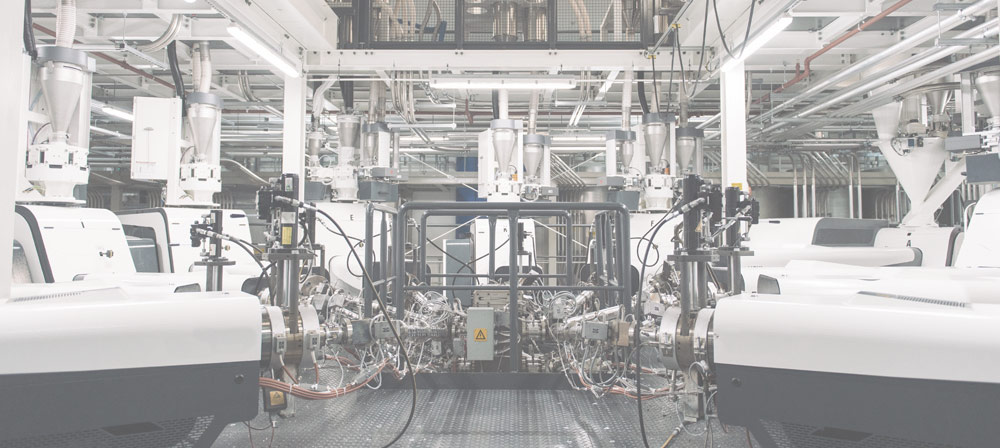
Through this investment, the Sligo site will feature Class 7 cleanroom manufacturing environments and state-of-the art thermoforming operations, fully certified to ISO 13485 standards and meeting the highest regulatory requirements.


Through this investment, the Sligo site will feature Class 7 cleanroom manufacturing environments and state-of-the art thermoforming operations, fully certified to ISO 13485 standards and meeting the highest regulatory requirements.

The Swedish electric vehicle battery manufacturer says it will construct a major new production facility in the city of Heide near Germany’s North Sea coastline.

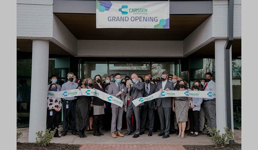
CARsgen Therapeutics 37,000-ft facility for clinical and early-stage commercial manufacturing was designed and built in just 12 months.
CAPE® is a transportable, tent-like cleanroom facility developed by researchers at the Fraunhofer Institute for Manufacturing Engineering and Automation IPA. It can be installed both indoors and in unexposed outdoor locations, and takes less than an hour to set up.
HTI Plastics recently received a new Krauss Maffei Injection molding machine for beta testing. The PX All-Electric arrived on our floor in late January. This is the second time HTI has been selected to host a Krauss machine for testing, with the option to purchase.
Bioquell offers a unique opportunity to broaden Ecolab’s portfolio of products, services, and solutions. Bioquell’s expertise in bio-decontamination and deep-cleaning utilizing vaporized hydrogen peroxide technologies complements Ecolab’s daily cleaning and disinfection offerings for cleanrooms and other high-grade environments.
The PSC filing, including a five-year capital investment overview and detailed one-year plan for 2019, sets forth the projects Ameren Missouri plans to implement to modernize energy grid infrastructure in Missouri to benefit its customers and offer them more tools to manage their energy usage.
Ten years into the future — that’s about how far UC Santa Barbara electrical and computer engineering professor John Bowers and his research team are reaching with the recent development of their mode-locked quantum dot lasers on silicon. It’s technology that not only can massively increase the data transmission capacity of data centers, telecommunications companies and network hardware products to come, but do so with high stability, low noise and the energy efficiency of silicon photonics.
QuantumClean & ChemTrace will demonstrate how its ultra-high purity chamber tool part cleaning, proprietary coatings and microcontamination analytical testing can help reduce wafer fabrication Cost-of-Ownership (CoO). Solutions’ information is available during show hours at SEMICON Europa at the Messe München Exhibition Center in Munich, Germany from November 13 — 16, 2018 (booth A4510).
The researchers created a new technology design for field effect transistors, which are basic switching devices in computers and other electronic devices. Those types of transistors also are promising candidates for next generation nanodevices. They can offer better switching behavior for computers and devices compared with traditional field effect transistors.
In a new study in the American Chemical Society journal ACS Nano, Rice materials scientist Jun Lou, graduate student and lead author Emily Hacopian and collaborators, including Tour, stress-tested rebar graphene and found that nanotube rebar diverted and bridged cracks that would otherwise propagate in unreinforced graphene.
SK hynix has grown into one of the leading chipmakers in the world through continuous effort to secure a fundamental competitive edge in the fierce semiconductor industry. With the emergence of new entrants and the consolidation of incumbent players, the competition and technological barriers are continuously heightening in the market.